Ion beam technology provides an exceptionally versatile approach to etch and deposition by offering a single tool and maximising system utilisation.
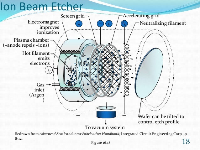
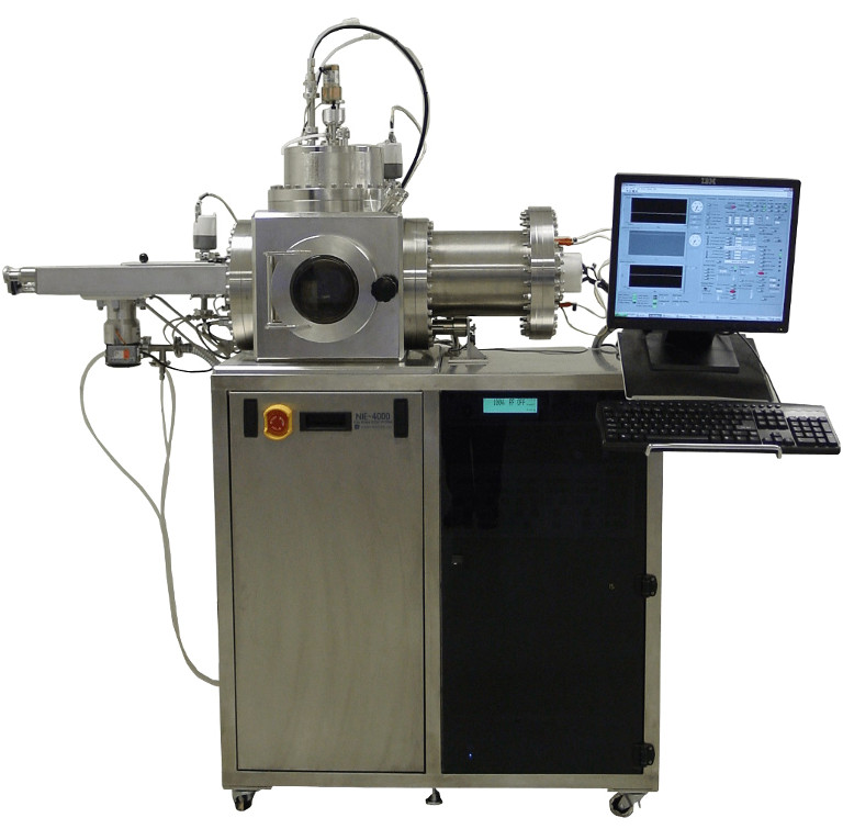
Ion beam etching system.
The ion beam figuring process now begins in the omf system.
Ion beam etching also known as ion beam milling or ion milling is the most widely used etching method for preparing solid state samples for scanning electron microscopy sem applications in this process the sample material is bombarded with high energy argon ion beams in a high vacuum chamber.
Full surface ion beam etching on 200 mm wafers the scia mill 200 is designed for structuring of complex multilayers of various materials.
This high value combination allows the customer to create thin film structures in common vacuum a significant value proposition compared to the competition.
Ion beam etch offers maximum flexibility coupled with excellent uniformity while ion beam deposition is ideal for its ability to produce deposited films with high quality dense and smooth surfaces.
A variety of sample holders and ion source configurations allow for a diverse range of applications to be carried out.
Reactive ion etching rie is an etching technology used in microfabrication rie is a type of dry etching which has different characteristics than wet etching rie uses chemically reactive plasma to remove material deposited on wafers the plasma is generated under low pressure by an electromagnetic field high energy ions from the plasma attack the wafer surface and react with it.
This determination process for the etching rate is necessary for all ion beam diameter.
With its fully reactive gas compatibility the system enables reactive etching processes with enhanced selectivity and rate.
Nano master s ion beam milling and etching systems are field proven fully automated systems that provide ease of use high reproducibility and reliable performance with extremely good uniformity.
A sample of the same material is used to determine the etching rate and set the source parameters.
For an exact process control different end point detection systems can be equipped.
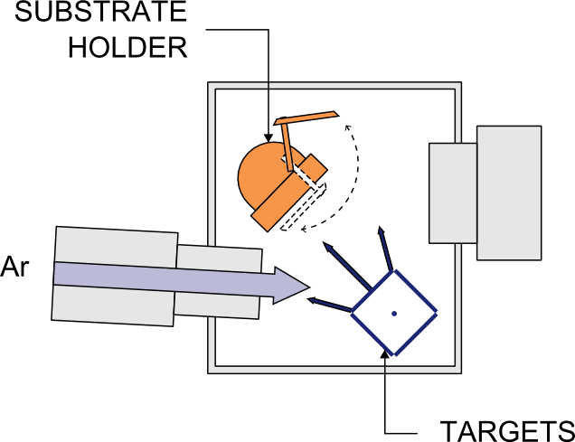
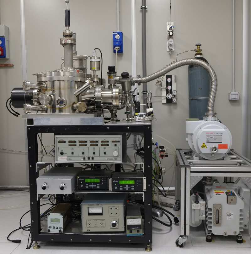
The basic dual ion beam sputtering dibs chamber set up as comprises an etching source that precisely directs a neutralised ion beam onto a wafer located in the substrate holder.
Normally for good uniformity the 15cm etch source can be used for wafers up to 4 while the 30cm etch source is suitable for wafers up to 8.
Oxford instruments is a leading provider of ibe technology systems.
System components such as shields are now easily accessible on the system itself.
Ion beam etching or milling is achieved by directing a beam of charged particles ions at a substrate with a suitably patterned mask in a high vacuum chamber.
The z flex system combines the best of ion beam etching and ion beam sputtering.

.jpg)